TPMC542

16/8 Channel Voltage & Current Range D/A and 20 Channel LVTTL/TTL Digital I/O

  • Standard single-width PMC module
  • 16 or 8 channel analog output
    • Single-ended
    • 16 bit D/A converter
    • Simultaneous update
    • 0 V … 5 V and 0 V … +10 V unipolar voltage ranges
    • ±5 V and ±10 V bipolar voltage ranges
    • 20% overrange possible for all voltage ranges
    • 0 mA … 20 mA, 0 mA … 24 mA and 4 mA … 20 mA current ranges
    • 20% over-range possible for all ranges
    • Sequencer mode available
    • Factory calibration data available in EEPROM
    • hardware correction function available
    • DMA support
  • 20 channel digital I/O
    • Tri-state 5 V-tolerant LVTTL/TTL
    • Pull resistors to 3.3 V, 5 V, GND
    • Input event detection
    • Input debounce filter
  • external synchronization trigger signals via P14 I/O
  • Front panel I/O (Mini D Ribbon (MDR68) type connector)

Product status: Active

Operating Temperature Range -40 °C to +85 °C RoHS compliant

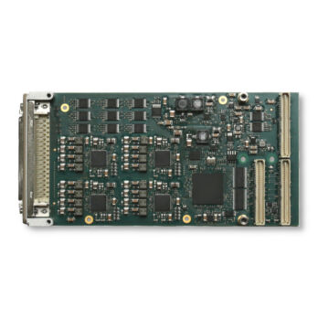
The TPMC542 is a standard single-wide PCI Mezzanine Card (PMC) compatible module providing 16 or 8 channels of simultaneous update single-ended unipolar/bipolar 16bit analog output and 20 channels of tristate capable 5V-tolerant LVTTL/TTL digital input/output.

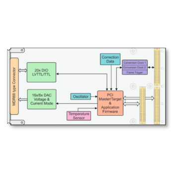
A 32 bit 33 MHz PCI interface is provided at the PMC P11 and P12 connectors. The digital I/O signals and analog output signals are accessible via a Mini D Ribbon (MDR68) type front I/O connector.

For each individual D/A channel, the following output ranges are configurable:

- 0V to 5V Voltage Range

- 0V to 10V Voltage Range

- ±5V Voltage Range

-  ±10V Voltage Range

- 4mA to 20mA Current Range

- 0mA to 20mA Current Range

- 0mA to 24mA Current Range

Additionally, for each Voltage Range a 20% over-range may be enabled.

The TPMC542 provides a D/A Sequencer unit for periodic simultaneous digital to analog conversions at a configurable conversion rate. In sequencer mode, the D/A conversion data is fetched from buffers in host memory by PCI master DMA transfer and is temporarily stored in an on-board data buffer. The Sequencer provides a Frame Mode used for repetitive frames of simultaneous D/A conversions upon an appropriate frame trigger signal event.

Conversion clock (conversion rate) and frame trigger signals may be generated on-board for internal use and may also be driven out on P14 rear I/O if the card is operating as a master card in a Multi-Board configuration. The conversion clock (conversion rate) and frame trigger signals may also be sourced externally via the P14 rear I/O interface if the card is operating as a target card in a Multi-Board configuration.

Each TPMC542 is factory calibrated. The correction data is stored in an on-board serial EEPROM unique to each PMC module. These correction values may be used to perform a hardware correction for every D/A channel and output range.

The digital I/O lines are ESD protected. Each digital I/O line has a dedicated line transmitter with individual output enable control and a dedicated line receiver. The line receivers are always enabled, so the digital I/O line level can always be monitored. Each digital I/O line input is capable of generating an interrupt triggered on rising edge, falling edge or both.

Additionally, a debounce filter can be configured to get rid of bouncing on the digital I/O inputs. Each digital I/O line has a 4.7k& pull resistor to a common reference. The common pull resistor reference is programmable by software (one setting for all digital I/O lines) to +3.3V, +5V or GND.
Mechanical Interface PCI Mezzanine Card (PMC) Interface confirming to IEEE P1386/P1386.1
Standard single-wide
Electrical Interface PCI Rev. 3.0 compatible; 33MHz / 32bit PCI; Initiator/Target; 3.3V and 5V PCI Signaling Voltage
FPGA Xilinx Spartan-6 FPGA
DAC AD5755-1ACPZ (Analog Devices)
Digital I/O 74LVT126PW (NXP)
FPGA Configuration Flash 32 Mbit Serial Flash, W25Q32FVZPIG (Winbond)
Correction Data EEPROM 16 kbit Serial EEPROM, M93C86-WMN6TP (ST)
D/A Channels TPMC542-10R: 16 D/A Channels
TPMC542-20R: 8 D/A Channels
D/A Channel

Output Range Options

Voltage Mode Ranges:
0V … 5V, 0V … 10V, -5V … +5V, -10V … +10V
Voltage Ranges available with 20% Overrange Mode:
0V … 6V, 0V … 12V, -6V … +6V, -12V … +12V
Up to 10mA load current per Voltage Mode D/A Channel
Current Mode Ranges:
4mA … 20mA, 0mA … 20mA, 0mA … 24mA
D/A Conversion Rate Max. 38ksps Conversion Rate (all D/A Channels simultaneous)
Digital I/O channels 20 TTL/LVTTL Digital I/O Lines
3.3V Driver, 5V tolerant Receiver, Individual Output Enable Control, Common Pull Resistor Reference Control (3.3V, 5V, GND)
Up to 15mA Source Current and up to 6mA Sink Current per Digital I/O Line
Front I/O 68-pin Mini D Ribbon (MDR) (3M N10268-52E2PC or compatible)
P14 Back I/O 64-pin Mezzanine Connector (Molex 71436-2864 or compatible)
Power Requirements Only the 5V PMC Power Supply is used
Typically 0.25A @ +5V DC without I/O Load
I/O Load Calculation:
Add 0.010A per active DIO Output Line
Add 0.070A per active D/A Voltage Output without Overrange
Add 0.082A per active D/A Voltage Output with Overrange
Add approx. (IRANGE_MAX2 * REXT) / 2.25V ampere per active D/A Current Output
Temperature Range Operating: -40°C to +85°C
Storage: -40°C to +85°C
Weight 1) 84 g to 92 g
Humidity 5 – 95% non-condensing
MTBF 1) 283 000 h to 356 000 h


1) depends on variant, for further details see User Manual

PRODUCT VARIATIONS

TPMC542-10R

16 Analog Voltage or Current Outputs (16 bit), 20 LVTTL/TTL I/O

16 analog outputs (voltage / current); 16 bit; simultaneous update; programmable ranges up to +/-12 V or up to 24 mA; 20 LVTTL/TTL I/O; factory calibrated; Front I/O via MDR68 connector

TPMC542-20R

8 Analog Voltage or Current Outputs (16 bit), 20 LVTTL/TTL I/O

8 analog outputs (voltage / current); 16 bit; simultaneous update; programmable ranges up to +/-12 V or up to 24 mA; 20 LVTTL/TTL I/O; factory calibrated; Front I/O via MDR68 connector

ACCESSORIES

MDR68 Cable

MDR68 Terminal Block

Cable Kit for Modules with MDR68 Connector

SOFTWARE

Device Driver for Multifunction Board Family (DAC, ADC and Digital I/O)

Data Sheet

Data Sheet

Data Sheet - Issue 1.0.3

User Manual

User Manual - Issue 1.0.3