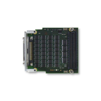
The TFMC684 is an FMC (FPGA Mezzanine Card) Mezzanine Module complying with the ANSI/VITA 57.1 standard that offers the possibility to add a 32bit M-LVDS (Multipoint Low Voltage Differential Signaling) I/O Interface or a 32bit RS-485/RS-422 I/O Interface to FMC Carrier Cards.
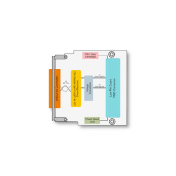
The Low Pin Count FMC Connector provides 32 independent control signals which configure the direction of each Differential Transceiver.
The 32 data lines are routed as single-ended traces from the FMC Connector to the Differential Transceivers where they are converted into 32 differential pairs.
The TFMC684-10R meets the TIA/EIA-899 standard (Type-2 Receivers) and the TFMC684-20R meets the TIA/EIA-485 and the TIA/EIA-422 standard.
The 32 bits of differential I/O are connected to a VHDCI-68 Connector in the front panel.
On every of the 32 bits the TFMC684-10R supports signaling rates up to 200Mbit/s which means that a 100MHz clock can be transmitted or in other words that 200M of voltage transitions per second can be performed. The TFMC684-20R supports signalling rates up to 16Mbit/s.
All signals connecting the Differential Driver/Receivers with the FMC Carrier are powered by an adjustable voltage generated by the Carrier. Because of voltage translation devices on the TFMC684 this voltage can range from 1.2V to 3.6V which allows the FPGA's I/O cells to be configured for various different I/O standards.
The signaling standard reference voltage pin, which is powered by the TFMC684, provides half of the adjustable voltage generated by the carrier for I/O standards requiring a reference voltage.
A power good LED indicates whether all voltages on the TFMC684, which are provided by the FMC Carrier, are within limits.
The TFMC684 is equipped with an I2C EEPROM which acts as an IPMI resource requesting the value of the adjustable voltage, for example.
The module meets the requirements to operate in extended temperature range from -40° to +85°C.


